Pages

Wednesday, 26 November 2014

The Basic of Logic Design ( Part 2 )

  
   SUM OF PRODUCT & PRODUCT OF SUM

Logic function can be written in a canonical form, where every input is either a true or complemented variable and there are only two levels of gates— one being AND and the other OR — with a possible inversion on the final output.

Two-level representation, and there are two forms, called sum of products and product of sums. A sum-of-products representation is a logical sum (OR) of products (terms using the AND operator) ; while a product of sums is just the opposite.

Example : Sum of Product

Example : Product of Sum 
E = ((A & B) + (A & C) + (B & C)) & (A & B & C )’
E = (A & B & C’ ) + (A & C & B’ ) + (B & C & A’ ) (SOP)

First equation has three levels of logic.

Second equation is in a sum-of-products form: 
 - It has two levels of logic and the only inversions are on individual variables.

Elaboration : We can also write E as a product of sums:

E =((A’ + B’ + C) & (A’ + C’ + B) & (B’ + C + A))’

Used De Morgan’s theorems to derive this form.

             ARITHMETIC LOGIC UNIT  (ALU)

An arithmetic logic unit (ALU) is a digital circuit used to perform arithmetic and logic operations.  It represents the fundamental building block of the central processing unit (CPU) of a computer. 

ALU – perform arithmetic and logic operation (addition, subtraction and logical operation: AND, OR)

Constructs an ALU from four hardware building blocks (AND and OR gates, inverts, and multiplexors) and illustrates how combinational logic works.

MIPS word is 32 bits wide, so need 32-bit-wide ALU (connect 32 1-bit ALUs ).

                                 1 Bit - ALU

  • This adder is called a full adder; it is also called a (3,2) adder because it has 3 inputs and 2 outputs. An adder with only the a and b inputs is called a (2,2) adder or half-adder.
  • The multiplexor on the right selects a AND b or a OR b, depending on whether the value of operation is 0 or 1. The line that controls the multiplexor is shown in color to distinguish it from the lines containing data.
  • An adder must have two inputs for the operands and a single-bit output for the sum.
  • There must be a second output to pass on the carry, called CarryOut. Since the CarryOut from the neighbor adder must be included as an input, we need a third input. This input is called CarryIn as shows in above diagram.
Specify the outputs of this ―black box‖ based on its inputs, as in truth tables.


  • The output functions Carry Out and Sum as logical equations, and these equations can in turn be implemented with logic gates.
  • Truth table shows the values of the inputs when CarryOut is a 1.
  • Turn this truth table into a logical equation:
          - CarryOut = (b & CarryIn) + (a & CarryIn) + (a & b) + (a & b * CarryIn)


Diagram below shows that the hardware within the adder black box for CarryOut consists of three AND gates and one OR gate. 

The three AND gates correspond exactly to the three parenthesized terms of the formula above for CarryOut, and the OR gate sums the three terms.

  • The sum bit is set when exactly one input is 1 or when all three inputs are 1.The sum results in a complex Boolean equation 
-sum = (a & b’ & CarryIn’ ) + (a’ & b & CarryIn’ ) + (a’ & b’ & CarryIn) + (a & b & CarryIn)

Diagram below shows a 1-bit ALU derived by combining the adder with the earlier components. Sometimes designers also want the ALU to perform a few more simple operations, such as generating 0. 
The easiest way to add an operation is to expand the multiplexor controlled by the Operation line and, for this example, to connect 0 directly to the new input of that expanded multiplexor.


Post by : Prema Santhini a/p Balasathiah (B031410001)

source 1 :  http://web.eecs.utk.edu/
source 2 :  Lecture Note Chapter 3

Tuesday, 25 November 2014

The Basic Of Logic Design (Part 1)

LOGIC DESIGN

1. Digital electronics operate with only two voltage levels:
    a high voltage and a low voltage.
2. Computer used binary system (1,0).
3. Combinational logic block contain no memory.
4. Logic block with n inputs, there are 2^n entries (possibility)
     in the truth table.


TRUTH TABLE

Consider a logic function with three inputs, A, B, and C, and three outputs,
D, E, and F. The function is defined as follows: D is true if at least one input is
true, E is true if exactly two inputs are true, and F is true only if all three inputs
are true. Show the truth table for this function.

The truth table will contain 2^3= 8 entries. Here it is:


Inputs
Outputs
A
B
C
D
E
F
0
0
0
0
0
0
0
0
1
1
0
0
0
1
0
1
0
0
0
1
1
1
1
0
1
0
0
1
0
0
1
0
1
1
1
0
1
1
0
1
1
0
1
1
1
1
0
1

Truth tables can completely describe any combinational logic function; however,
they grow in size quickly and may not be easy to understand. Sometimes we want
to construct a logic function that will be 0 for many input combinations, and we
use a shorthand of specifying only the truth table entries for the non-zero outputs. 


BOOLEAN ALGEBRA

Another approach is to express the logic function with logic equations. 


1. The OR operator is written as +, as in A + B
o   0 + 1 = 1 ------- 1 + 0 = 1
2. The AND operator is written as & , as in A & B
  o   0 · 1 = 0 ------- 1 · 0 = 0
3. The NOT (inversion) operator is written as - or ' , as in A'
  o   0’ = 1 ------- 1’ = 0

BOOLEAN ALGEBRA LAWS

CLASSIFICATION
LAWS
Identity
A + 0 = A
A & 1 = A
Zero and One
A + = 1
A & 0 = 0
Inverse
A + A’ = 1
A & A’ = 1
Commutative
A + B = B + A
A & B = B & A
Associative
A + (B + C) = (A + B) + C
A & (B & C) = (A & B) & C
Distributive
A & (B + C) = (A & B) + (A & C)
A + (B & C) = (A + B) & (A + C)
Demorgan’s
(A + B)’ = A’B’
(AB)’ = A’ + B’

GATES

1. Logic blocks are built from gates that implement basic logic functions.
2. Any logical function can be constructed using AND gates, OR gates, and inversion.
3. Two common inverting gates are called NOR and NAND.


DECODER


1. Use decoder to build larger components
2. The most common type of decoder has an n-bit input and 2^n outputs, where only one output is asserted for each input combination.

3. This decoder translates the n-bit input into a signal that corresponds to the binary value   of the n-bit input.
4. The outputs are shows a 3-bit decoder and the truth table. This decoder is called a 3-to-8 decoder.
5. Since there are 3 inputs and 8 (2^3) outputs. There is also a logic element called an
6. Encoder that performs the inverse function of a decoder, taking n inputs and producing
7. an n-bit output.


                                 A 3-bit decoder and the truth table for a 3-bit decoder


A 3-bit decoder has 3 inputs, called 12, 11, and 10, and 2^3 = 8 outputs, called Out0 to Out7. Only the output cor responding to the binary value of the input is true, as shown in the truth table. The label 3 on the input to the decoder says that the input signal is 3 bits wide. 


MULTIPLEXOR (SELECTOR)

The output is one of the inputs that is selected by a control
The left side shows this multiplexor has three inputs:
two data values and a selector  (or control) value. The selector value determines which of the inputs becomes the output. We can represent the logic function computed by a two-input multiplexor, shown in gate form on the right side as C = (A & S') + (B & S)


  • Multiplexors can be created with an arbitrary number of data inputs. 
  • When there are only two inputs, the selector is a single signal that selects one of the inputs
  • if it is true (1) and the other if it is false (0). If there are n data inputs, there will need to be [log2 n] selector inputs. 
  • In this case, the multiplexor basically consists of three parts:

1. A decoder that generates n signals, each indicating a different input value
2. An array of n AND gates, each combining one of the inputs with a signal
from the decoder
3. A single large OR gate that incorporates the outputs of the AND gates


  • To associate the inputs with selector values, we often label the data inputs numerically (i.e., 0, 1, 2, 3, . . . , n − 1) and interpret the data selector inputs as a binarynumber. 
  • Sometimes, we make use of a multiplexor with undecoded selector signals.
  • Multiplexors are easily represented combinationally in Verilog by using if expressions.
  • For larger multiplexors, case statements are more convenient, but care must be taken to synthesize combinational logic.

Sourceshttp://www.cs.colostate.edu/
                http://cs.baylor.edu/
                Lecture note chapter 3

Post by : Ain Nasuha Bt Abdul Yazid


Friday, 21 November 2014

LANGUAGES OF THE COMPUTER 2 PART 1 (DECODING MACHINE LANGUAGE)

Decoding Machine Language

-----> six machine language instructions in hexadecimal:
     00001025hex   

  0005402Ahex
                                                         
  11000003hex
                                                
  00441020hex

  20A5FFFFhex 

  08100001hex
1.Firstly we must  convert hex to binary

00001025hex   = 00000000000000000001000000100101
0005402Ahex  =   00000000000001010100000000101010
11000003hex    =  00010001000000000000000000000011 
00441020hex  =   00000000010001000001000000100000
20A5FFFFhex  = 00100000101001011111111111111111
08100001hex  =   00001000000100000000000000000001

2.Ok,after tahat we identify the  opcode and format


*** Here some tips to identify which format should we use ( ^ _ ^ )


 Look at opcode:

  ***which is first 6 bits  of the binary number

[ 000000] 00000000000001000000100101

[ 000000] 00000001010100000000101010

[ 000100] 01000000000000000000000011

[ 000000] 00010001000001000000100000

[ 001000] 00101001011111111111111111 

[ 000010] 00000100000000000000000001

 0   ------> R-Format

2 or 3 ------> J-Format

 otherwise------>  I-Format


0
rs
rt
rd
shamt
funct
    1,4-31
rs
rt
immediate
2 or 3
Target address
op = 6 bits
rs  = 5bits
rd = 5bits
shamt = 5 bits
funct = 6 bits
immediate = 16 bits
address = 26 bits

Ok , got it?Lets continue the next step!!!!

3.Translate  to MIPS assembly instructions.
        or $v0 , $0 , $0
loop :  $v0 , $0 ,$a1
         beq $t0  , $0 , Exit
         add $v0  ,$v0  , $a0
         addi $a1 , $a1 , -1
          j Loop
Exit


Ok done!!
post by; Nursyahirah Syafiqah binti Baharim

ABOUT US


UMMI IZZATI MUSTAPHA
"Success seems to be connected with action. Successful people keep moving.They make mistakes,but they don't quit"


AIN NASUHA ABDUL YAZID 

"If you are not wiling to learn, no one can help you. If you are determined to learn, no one can stop you." -Anonymous


PREMA SANTHINI A/P BALASATHIAH

“Be a student as long as you still have something to learn, and this will mean all your life.”
Henry L. Doherty


AYUNI NADIRAH BINTI ABD NASIR

"If plan A didn't work. The alphabet has 25 more letters. Stay cool."

NURSYAHIRAH SYAFIQAH BINTI BAHARIM


“Success does not depend on your aptitude or your altitude. It depends on your attitude.”

INPUT / OUTPUT (PART 2)


I/O - Input/Output


IOPS - I/O (Input/Output) operations per second

Input/Output Adapter


BIOS - Basic Input/Output System


The ROM BIOS Explained


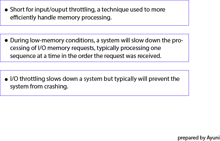
Input/Output Throttling


Source:
http://en.wikipedia.org/wiki/Peripheral
http://www.webopedia.com/


Posted by AYUNI NADIRAH BINTI ABD NASIR